Nanocrystal electronics
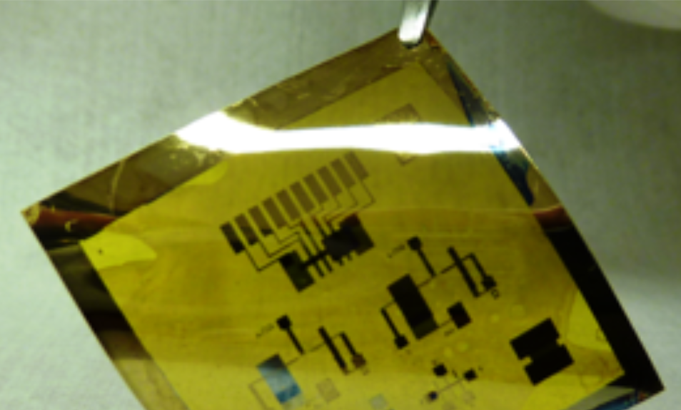
Colloidal semiconductor nanocrystals and nanowires present an exciting new class of solution-processable materials for the low-cost, large-area fabrication of flexible, thin film electronics. In the Kagan group, we study the role of surface chemistry on processability and nanocrystal coupling, passivation and doping and develop fabrication methods to construct and tailor the characteristics of electronic devices and circuits from colloidal nanocrystal inks. We design more complex integrated, flexible nanocrystal circuits for a growing number of electronic and sensing applications.
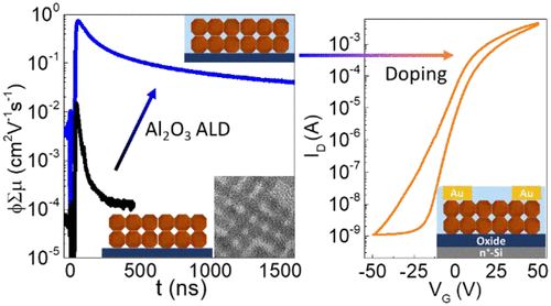
Enhanced Carrier Transport in Strongly Coupled, Epitaxially Fused CdSe Nanocrystal Solids Journal Article
In: Nano Letters, vol. 21, no. 7, pp. 3318–3324, 2021.
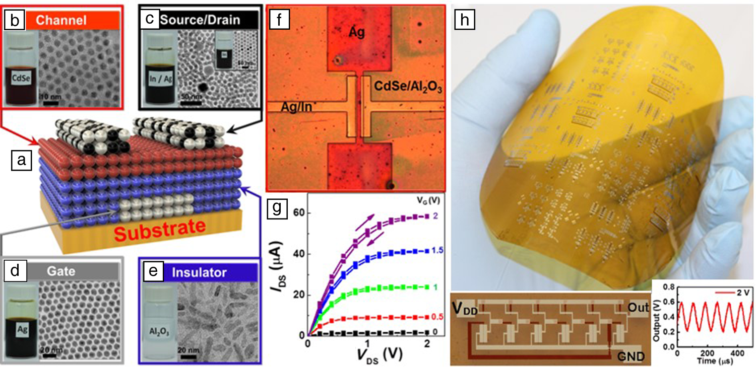
Self-assembly for electronics Journal Article
In: MRS Bulletin, vol. 45, pp. 807–814, 2020.
Optical metamaterials
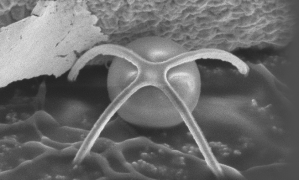
Subwavelength metal and highly-doped semiconductor structures support surface plasmons: collective oscillations of the delocalized electrons in the material upon interaction with light. In the Kagan group, we construct plasmonic structures through both top-down nanofabrication from bulk materials and bottom-up assembly from nanocrystal building blocks. We apply plasmonic nanostructures 1) to utilize their strong electromagnetic fields to enhance absorption, charge separation and photoluminescence in organic and inorganic materials and their devices and 2) as building blocks in the construction of large-area, broadband, tunable optical metamaterials.
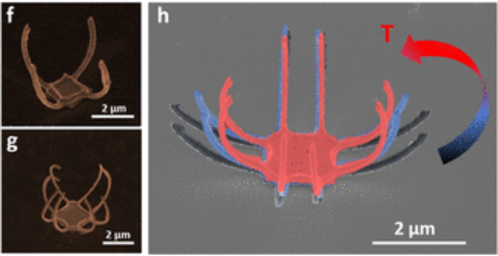
Chemo- and Thermomechanically Configurable 3D Optical Metamaterials Constructed from Colloidal Nanocrystal Assemblies Journal Article
In: ACS Nano, vol. 14, no. 2, pp. 1427-1435, 2019.
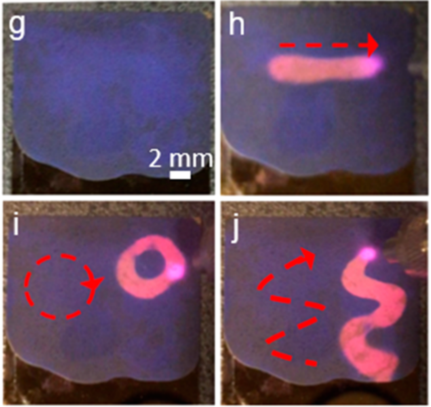
Designing Strong Optical Absorbers via Continuous Tuning of Interparticle Interaction in Colloidal Gold Nanocrystal Assemblies Journal Article
In: ACS Nano, vol. 13, no. 7, pp. 7493-7501, 2019.
Synthesis and assembly of colloidal nanocrystals
Tunable synthesis and assembly of colloidal nanocrystals has allowed us to prepare new materials which enable a wide variety of sensing and communication applications, overcoming fabrication and environmental constraints which apply to more traditional bulk materials. By controlling the diameters of nanocrystals during synthesis, we create quantum dots with tunable photoluminescence properties that are determined by confinement effects. By controlling the stoichiometry of nanocrystal thin films, we control the carrier statistics and polarity of charge transport in nanocrystal thin film solids. By controlling the stabilizing ligands on the surfaces of colloidal nanocrystals, we can control their assembly and arrangement in thin films and thereby control the plasmonic and electronic properties of the films as well. Furthermore, using templated assembly methods, we can position nanostructures with various shapes and sizes according to their individual physical properties to create large-area metamaterials or multifunctional nanomaterials. For example, a templated assembly of structures may exhibit a chiral light sensitivity which no individual particle exhibits, and quantum dots co-assembled with plasmonic nanoparticles may exhibit enhanced optical properties.
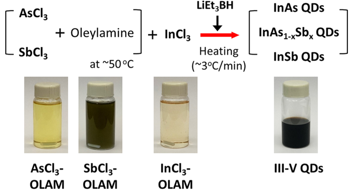
General Synthetic Route to High-Quality Colloidal III–V Semiconductor Quantum Dots Based on Pnictogen Chlorides Journal Article
In: Journal of the American Chemical Society, vol. 141, no. 38, pp. 15145-15152, 2019.
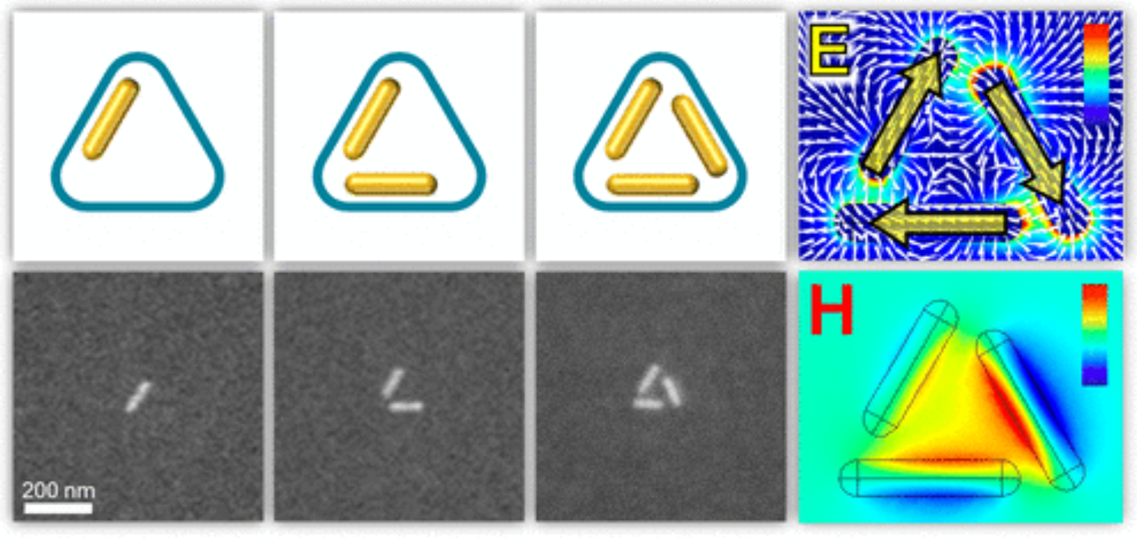
Plasmonic Optical and Chiroptical Response of Self-Assembled Au Nanorod Equilateral Trimers Journal Article
In: ACS Nano, vol. 13, no. 2, pp. 1617–1624, 2019.
2D Perovskite Photophysics
Nanocrystal assemblies have been coined “artificial solids.” Charge injection and transport is of fundamental interest, to understand the cooperative interactions that develop and the delocalization of quantum confined electronic wavefunctions as nanocrystal building blocks are brought into increasingly strong coupling in the solid state. Transport studies are also of technological importance, as semiconductor nanocrystals are promising for a range of electronic, optoelectronic and thermoelectric applications. In the Kagan group, we use a wide range of electronic and optical spectroscopies to probe the nature and evolution of charge transport in nanocrystal thin films as we use ligand exchange chemistries, to control the interparticle distance and the strength of electronic coupling, and surface chemical modification, to passivate surface states and dope the nanocrystal thin films.
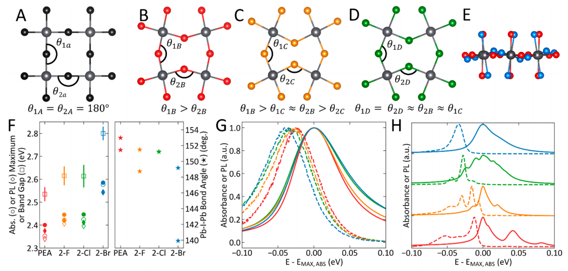
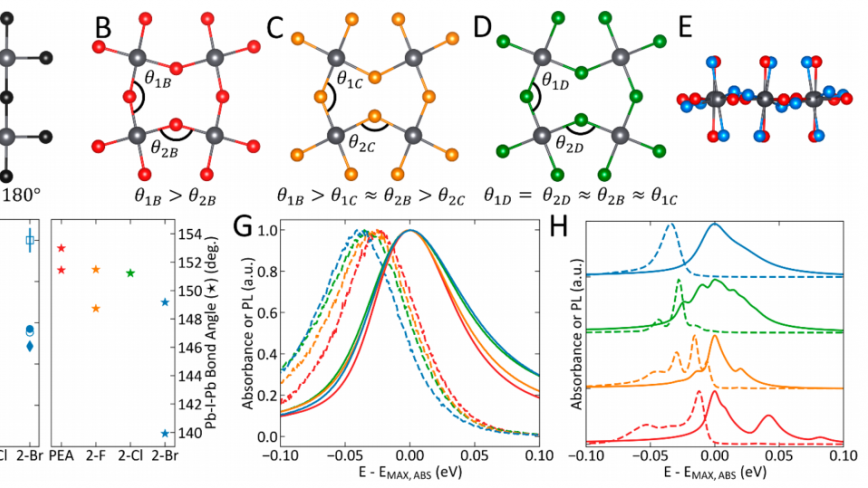
Tailoring Hot Exciton Dynamics in 2D Hybrid Perovskites through Cation Modification Journal Article
In: ACS Nano, vol. 14, no. 3, pp. 3621–3629, 2020.
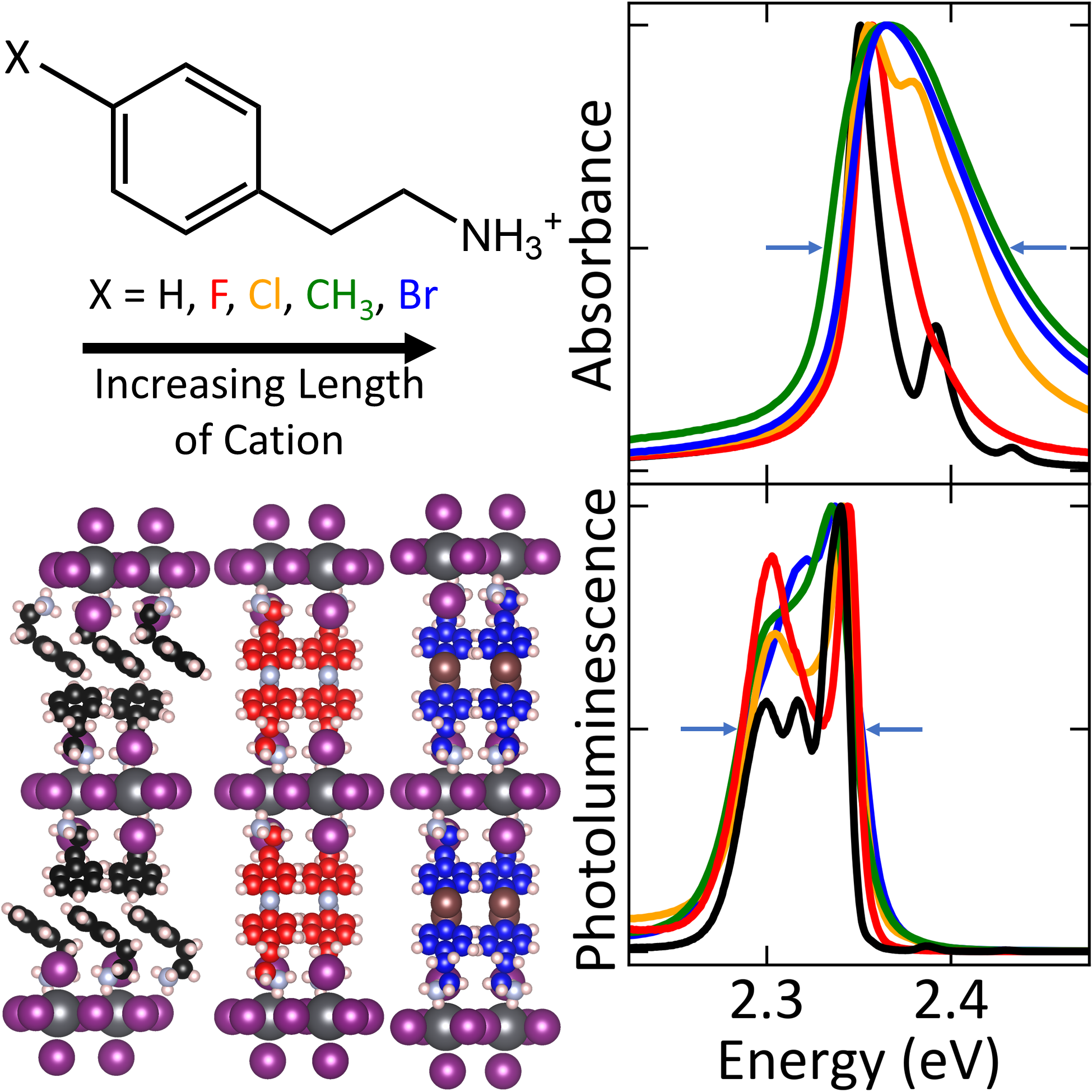
Longer Cations Increase Energetic Disorder in Excitonic 2D Hybrid Perovskites Journal Article
In: Journal of Physical Chemistry Letters, vol. 10, no. 6, pp. 1198–1205, 2019.
